
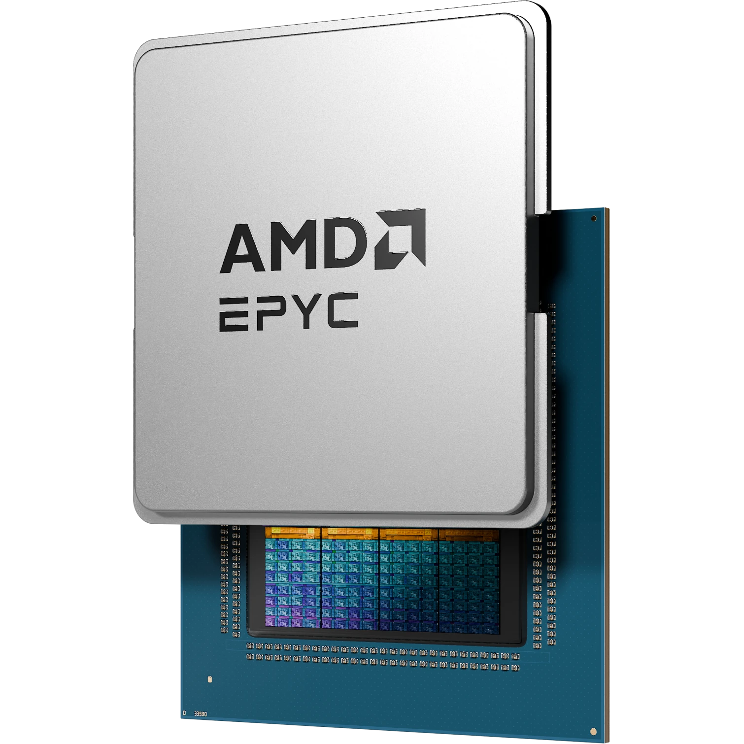
AMD has revealed the first models of its sixth-generation Epyc product line, Venice. Based on the new Zen 6 and Zen 6c cores, the now-shipping processors offer two packaging options. Maximum core count increases from 192 in the previous Turin generation to 256. As before, the highest-frequency chips boost to 5 GHz. Across the board, peak memory throughput is more than double that of Turin.
Since AMD launched the first Epyc server processors in 2017, the company has expanded from a challenger targeting hyperscalers into a broad supplier addressing enterprise, telco, and other markets. Now the company must also address AI systems, offering GPU hosts and Epyc configurations for AI agents’ applications. Consequently, the sixth-generation Epyc lineup spans multiple families and products varying in core density, cache size, memory throughput, and I/O capabilities. Thankfully, AMD has avoided Intel’s segmentation excesses and accompanying SKU proliferation.
AMD Epyc 9006 Venice Product-Line Overview
The sixth Epyc generation comprises four families:
- 9006 SP7
- 9006 SP8
- 9006X SP7
- 9006 LP
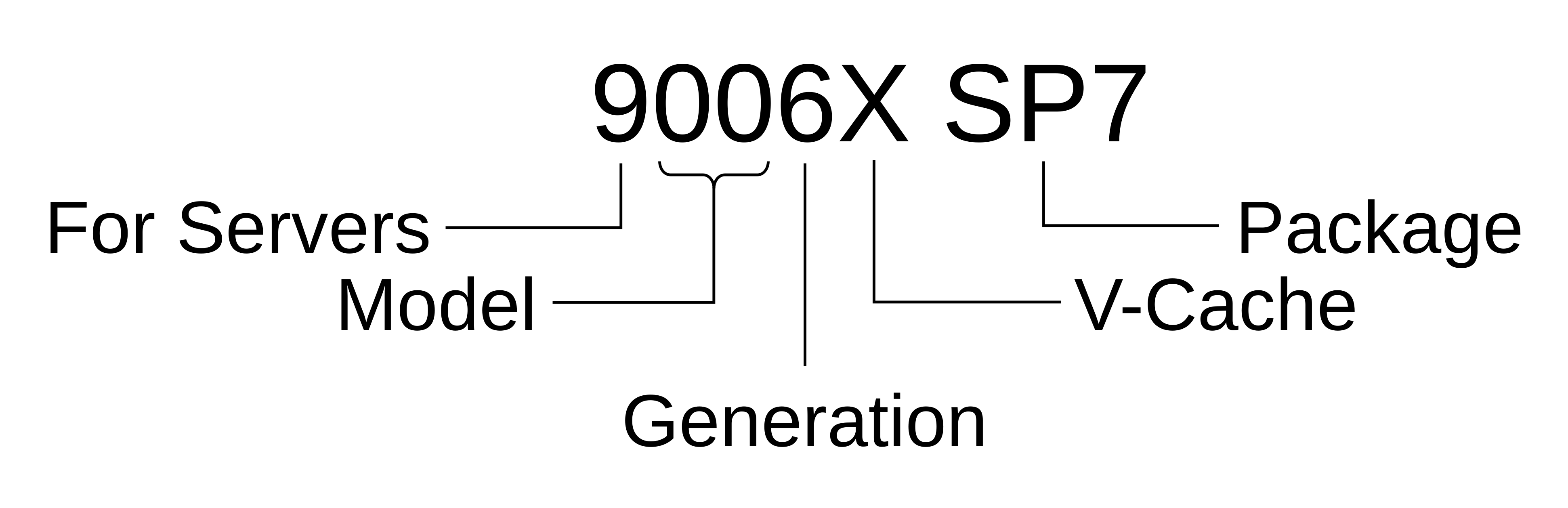
Mainline Epyc processors have names starting with a 9, and the ending digit indicates the generation, as Figure 1 shows. The SP7 and SP8 codes designate the package type. Integrating two I/O dice, the SP7 processors have 16 DDR5 DRAM channels and 96 PCIe lanes. The smaller SP8 chips halve the number of DRAM channels and raise the PCIe lane count to 128. The 9006X processors will stack compute and cache dice to enlarge the L3 cache. The lower-power LP models employ yet a different package and feature LPDDR5X instead of DDR5 memory interfaces.
Epyc 9006 SP7 Models: Core Counts and DDR5 Interfacing
Shipping next quarter, the SP7 models scale to 256 cores and provide 16 DDR5 interfaces. As it did with the fifth-generation Turin processors, AMD doesn’t conspicuously distinguish between models using the physically compact, lower-clocking, lower-power Zen 6c and the high-performance Zen 6 (non-c) core. However, whereas the Zen 5 (non-c) Turins scale to 128 cores, the Zen 6 Venices scale to only 96.
Epyc 9006 SP8 Models: Core Density and Telco-Use Suitability
In past generations, AMD had “NEBS-friendly” (i.e., compliant with telco thermal requirements) Epycs housed in a smaller package and coded as the 8000 series. The SP8 models fulfill the same role in the sixth generation but share the Venice designation and 9006 naming scheme of their larger-packaged stablemates. In so doing, AMD conveys that these chips aren’t lesser, only different. The Epyc 9016 has the fewest cores in the Venice lineup, eight, to address designs, such as storage, requiring PCIe and DRAM throughput but little computation. The densest SP8 models have 128 cores. AMD plans to start shipping the SP8 models in 1H27.
3D V-Cache and Other Cache-Size Options
Because AMD assembles Epyc processors from chiplets, each combining CPU cores and L3 cache, cache size scales with core count. By integrating 8 computing dice, each with 32 Zen 6c cores and 128 MB of L3 cache, the 256-core Epyc 9996 amasses a correspondingly capacious 1 GB L3 cache. Conversely, models with fewer CPUs, constructed by packaging fewer compute chiplets, have smaller L3 caches. AMD, however, has the option to deactivate cores within a chiplet to reduce the number while maintaining L3 cache size. For example, the Epyc 9176F has only 16 Zen 6 cores but sports an L3 cache of 192 MB, indicating that this model employs four computing dice, each contributing only four of its 12 cores and all of its 48 MB L3 cache.
The customers requiring the most DRAM bandwidth and the largest caches also require the faster Zen 6 cores. AMD is therefore replicating its past product strategy of stacking compute and cache chiplets, which the company calls 3D V-Cache. The flagship Epyc 9006X model will add cache dice to the 96-core Zen 6 SP7 configuration, raising its L3 cache to 1,152 MB. However, AMD has yet to disclose specific 9006X models, which it plans to ship in 2H27.
Epyc 9006 LP (Verano) LPDDR5X and GPU Interfaces
The LP models adapt the Epyc design for GPU-adjacent applications. Called Verano, not Venice, these Zen 6 processors integrate LPDDR5X memory interfaces instead of DDR5. They also feature AMD’s proprietary XGMI interface (not to be confused with XGMII) employed by its GPUs. The company has yet to disclose whether it’s designing only a new I/O die or a monolithic chip combining processing and I/O functions. Verano is similar in core density, DRAM interfacing, and proprietary I/O to the Nvidia Vera and Grace processors. Set to ship in 2H27, Verano will be the GPU host in the next-generation Helios 500.
Zen 6 Microarchitecture, IPC, Frequency, and DRAM Bandwidth
Although AMD has withheld the Zen 6 microarchitecture, initial performance disclosures suggest that Venice could raise instruction throughput (IPC) by 20% over Turin. We expect the Zen 6 microarchitecture to implement many incremental changes to the Zen 5 design, which could account for half of Epyc’s IPC increase.
Additional IPC gains come from an improved memory hierarchy. As alluded to above, a Zen 6c chiplet provides 4 MB of L3 cache per core (assuming none are deactivated), up from only 2 MB for its Zen 5c predecessor and the same amount as the Zen 6 and Zen 5 chiplets. More significantly, the SP7 designs increase DRAM throughput by 2.7× the fifth-generation Epyc’s peak. These chips raise transfer rates and feature 16 DRAM channels compared with Turin’s maximum of 12. Moreover, they support MRDIMMs, which further raises throughput. The MRDIMM standard addresses the bottleneck in DDR5 memory: writing/reading memory to/from the DRAM array. It puts two ranks (sets of memory chips) on each DIMM, interleaving their data. This enables the memory interface to operate at 12,800 MT/s, twice Turin’s rate.
Clock-rate comparisons are challenging, even after AMD’s disclosure of more than two dozen models. The company specifies boost and base rates, which it limits to constrain temperature and power. As with Turin, the fastest available boosted rate is 5 GHz. However, Venice offers this rate on a 96-core model compared with only 64 cores for the densest 5 GHz Turin. For the SP8 packaging option, to hold the new chip to its predecessor’s 400 W limit, AMD reduced the base clock from 3.3 GHz to 3.1 GHz. For customers with a 500 W power budget, AMD offers the Epyc 9686F. A 96-core chip in the SP7 package, it boosts to 5 GHz and has a 3.4 GHz base clock. These options exemplify how, throughout the Venice portfolio, AMD makes various tradeoffs compared with Turin. For example, Venice offers more cores in the same power budget but at a reduced clock rate. Similarly, other models offer the same core count at the same base clock rate but at reduced power.
Comparing Venice with Intel Xeon 6/6+ and Nvidia Vera
Intel has been AMD’s main competition but is outclassed. Its Xeon 6 performance-core series (Granite Rapids) launched in 2024, scaling to fewer cores than the contemporaneous Turin. Its successor, Diamond Rapids, is due in 2027. To serve customers requiring greater core density, Intel recently launched its Xeon 6+ (Clearwater Forest) line, which provides 144–288 efficiency cores. However, these E-cores don’t match the Zen 6c’s IPC or clock rate. A diminished competitor, Intel remains a major force owing to its customer base and the burgeoning market demand for server processors.
Nvidia is a rising competitor but has a limited product line. We expect to see few instances where customers will compare the company’s newest CPU, the Arm-compatible Vera, with Venice. AMD can offer similar memory bandwidth per core but using DDR5 instead of Vera’s LPDDR5X, and AMD provides x86 compatibility. A more straightforward comparison is due next year when AMD ships Verano, which also employs LPDDR5X. For now, Nvidia poses a limited threat.
Epyc Roadmap: Future Zen 7 and Zen 8 Designs and Target Availability
Beyond Venice, AMD outlined its server-processor roadmap, promising a two-year product cadence. Due in 2028, Zen 7 will introduce a new architecture on a new process node, presumably a 16 Å or 14 Å technology, and debut the x86 AI Compute Extensions (ACE). Two years later, AMD will produce Zen 8, which the company has already started developing. The code name for the next-generation Epyc processors is Florence, and its successor is Ravenna.
Bottom Line
AMD is the most consequential server-processor supplier in 2026 and is set to deliver a broad line of sixth-generation Epyc chips. Venice coalesces the company’s different core types and packages into a unified product line. Simultaneously, AMD continues to deliver a variety of options to meet customers’ varying requirements. The flagship Epyc model integrates more high-performance cores than any other CPU and sets a high-water mark for cache size and DRAM throughput. Over the past 10 years, AMD has transformed from the data-center CPU challenger, addressing the growing cloud business by pushing core-density limits, to the incumbent offering a broad line comprising options for multiple markets. In its new role, AMD must be mindful of a fleet-footed challenger stealing a march by capitalizing on an emerging trend.