Nvidia has disclosed the first Blackwell (B100/B200) details, promising performance gains from 3× to 30× over Hopper (H100/H200). The new chip’s raw performance is about 2.5× that of its predecessor. Just as muscle-car enthusiasts know there’s no replacement for displacement, Nvidia accomplished these gains by using 2.5× more transistors. The first Nvidia Blackwell shipments are to occur this year, but it will be 2025 before volume ramps.
Notables
- Timing—Nvidia understandably wanted to make a big announcement at its GTC conference, but the company could be seen as taking a risk by preannouncing Blackwell, especially with Hopper lead times approaching normal. However, the lead time for engaging with major customers is long for complex data-center products like GPUs/NPUs.
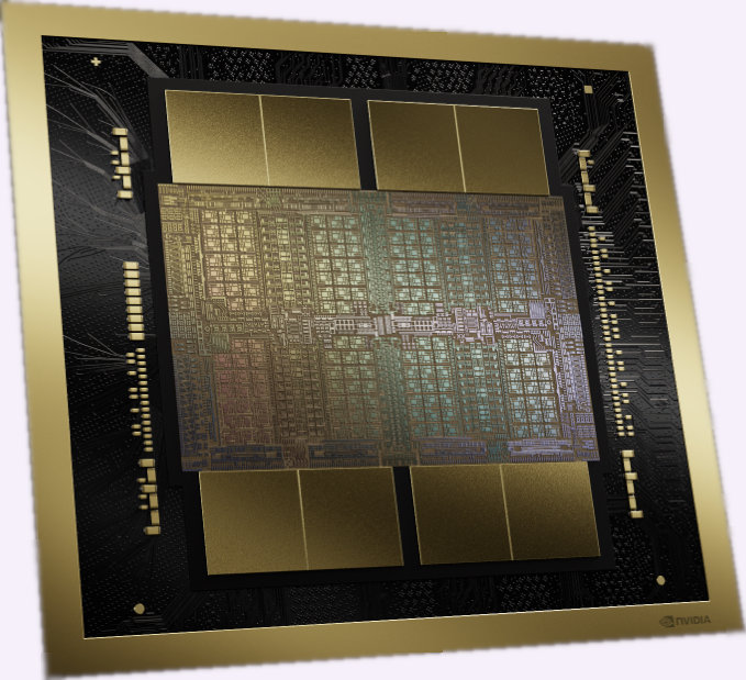
- Chiplets—Nvidia Blackwell increases transistor count by employing two logic dice, each with more transistors than one H100 logic die. Owing to their size and resulting low yields, they’ll be expensive to manufacture. We estimate that if Blackwell’s die yield is 45%, dividing the die in two (i.e., employing four 440 mm2 dice instead of two 860 mm2 dice) would raise yield to 64%. Because using more, smaller dice would likely reduce total manufacturing cost, we doubt Nvidia’s claim that there’s no performance penalty from chiplets compared with a monolithic design.
- Process technology—Blackwell’s TSMC 4NP process is likely Nvidia’s version of the foundry’s N4P technology. The 4NP process likely adds metal layers to the standard N4P recipe and should be incrementally better than Hopper’s 4N process, but its use casts doubt on TSMC’s 3 nm generation, at least for huge dice.
- Power—Like the H100, the B100 is a 700 watt chip. The B200, however, operates at a full kilowatt. Based on published power and performance figures, it appears that the B100 and B200 are the same silicon, but the former operates at 75% of the B200’s clock rate.
- Memory and interface upgrades—In adding computational resources, Blackwell has more than twice the HBM capacity and memory-interface speed of the H100. (It’s also an improvement over the H200, which upgrades the H100’s HBM to the newer HBM 3e used in Blackwell.) NVLink and PCIe speeds also double to feed the chip’s voracious data appetite.
- Number format—one of Blackwell’s new features is FP4 support. Applicable to inferencing, not training, FP4 throughput (flops) is twice that of FP8. The smaller type also doubles memory capacity and interface throughput (measured in words, not bits). Providing only one mantissa and two exponent bits, FP4 is weird. Like block-floating-point formats, FP4 also has a separate scaling factor applying to a data group. Although FP4 isn’t universally applicable, it will speed up some models. Note that when Nvidia talks about its Transformer Engine, it’s referring to a combination of its tensor (matrix) units and software; much of Blackwell’s Transformer Engine’s speedup comes from employing these new, smaller data types.
- Performance—Nvidia peppers its Blackwell collateral with a lot of performance claims. The easiest to grok is the claim that a cluster of B200-based HGX systems will be 3× faster than the same-sized H100-based HGX cluster, which is consistent with Blackwell’s added raw throughput and interface speeds. The company projects inference throughput on the GPT-MoE-1.8T model will increase 15× compared with the H100. Note that this is per GPU for HGX clusters. We estimate that 2.5× comes from Blackwell’s bigger size, and another 2× comes from employing FP4. The remaining 3× mostly derives from how Blackwell’s greater resources reduce the amount of data shuffled among GPUs and between GPUs and off-chip memory and from the new chip’s faster interfaces. The headline 30× speedup is also per GPU for GPT-MoE-1.8T inferencing but compares an H100 HGX cluster to the GB200 NVL36, which is a rack-scale system containing 18 Grace Blackwell “superchips.” These modules combine Nvidia’s Grace processor with two B200s. The GB200’s performance doubling over the HGX board results from the fast CPU-GPU interfaces, which accelerate loading data into the GPUs.
Competition
Nvidia has raised the performance bar, forcing competitors to compare their forthcoming AI accelerators with Blackwell, not Hopper. Ramping this year, the AMD MI300X has 30% greater raw (theoretical peak) execution rate than the H100 but will be dwarfed by Blackwell come 2025. The AMD MI400 must make as big a leap over its predecessor as Blackwell does. The other big lurking rival is Intel, which seeks to reboot its data-center-accelerator business with Falcon Shores, which it will follow with Falcon Shores 2 in 2026. Employing the company’s 18A or 20A process, Falcon Shores may have a power and silicon-cost advantage over Blackwell. It’s likely to employ a complex, expensive package like Intel Ponte Vecchio—but this may be what it takes to scale it out to Blackwell-level performance. By the time AMD and Intel start shipping their products, however, Nvidia may have announced its next data-center architecture, Rubin.
However, by scaling out performance while delivering lesser gains in power efficiency, Nvidia opens its flank. Big GPUs/NPUs are better for big models, but billion-parameter (and smaller) models won’t experience the same gains that Nvidia shows for Blackwell on GPT-MoE-1.8T. Chips like the Tenstorrent Grayskull that promise better power and cost efficiency than Blackwell or Nvidia’s less-exotic cards (e.g., the L40) may be able to carve out a niche, especially in inferencing systems, which are smaller than those for training.
Customers
Because everyone knows that world+dog uses Nvidia’s AI products, it’s less important for the company to trot out endorsements than for its challengers. For the Blackwell launch, however, Nvidia provided a supporting-quote list that underscored its position in the industry. Not only does the list include each of the Magnificent Seven (sans Apple) and others, the quotes are from CEOs.
Customers training the largest models will get the most value from Blackwell, but those requiring only a single eight-GPU HGX system will still benefit from its performance uplift. Sourcing from Nvidia has the added advantage that the company generally supports unusual features such as FP4 relatively well. Developing its own systems and networking technology, Nvidia also wrings out integration and scaling issues, enabling its chips to deliver real-world gains commensurate with theoretical improvements. In short, setting aside costs (capex and opex), Blackwell delivers more of what customers want from Nvidia.
Bottom Line
More than doubling Hopper’s already-prodigious silicon budget, the Nvidia Blackwell is a big chip. Most customers will find its per-GPU performance increases proportionately. Although in some cases—particularly trillion-parameter-model inferencing—the speedup could be greater, customers should not generally expect to see the 15× (much less 30×) gains the company has highlighted. Moreover, few Blackwell systems will be available before the end of the year. Finally, a 1.0 kW chip isn’t for every data-center application, leaving opportunities for competitors. Those, however, seeking to challenge Nvidia’s performance may need to recalibrate their product plans.
Comments
One response to “Nvidia Blackwell GPU Promises 30× Speedup, but Expect 3×”
When I write “if Blackwell’s die yield is 45%, ” I’m posing a hypothetical. However, it might be more realistic to assume yield is higher. Chips like Blackwell lend themselves to adding redundancy to cope with defects.