Last week Google revealed its seventh-generation TPU, the company’s name for its AI processors (NPUs). Dubbed Ironwood and due to be available to Google Cloud customers by the end of the year, it promises much more peak throughput than past TPUs—about 10× more TFLOPS than the TPU v5p.
Notable Google TPU v7 (Ironwood) Attributes
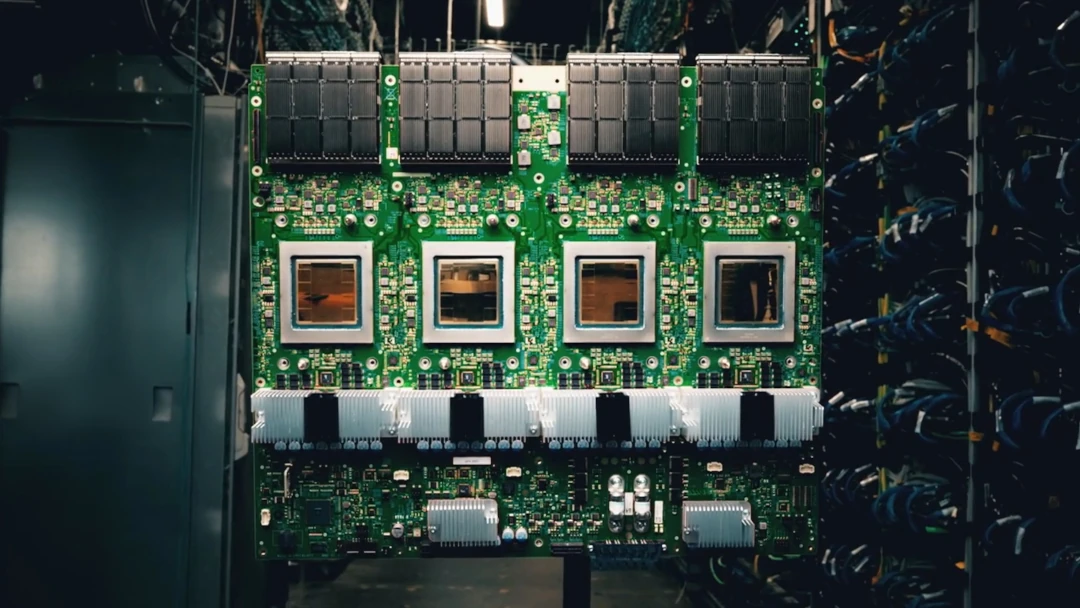
- Architecture—The TPU is unusual, employing only one or two VLIW computing cores divided into scalar, vector, and two or four matrix units. The lattermost MXUs provide most of the computing power. The design bears a passing resemblance to that of Intel Gaudi.
- MXUs—Most TPU generations’ MXUs employed 128×128 multiply-accumulate (MAC) arrays, improving source-code compatibility among generations. Breaking with previous gens, Google Trillium (TPU v6) doubled each dimension, quadrupling per-cycle MAC throughput. We infer that Ironwood carries forward Trillium’s 256×256 arrangement for 16-bit operations, delivering a 4× per-cycle speedup compared with the v5p’s MXU design.
- Precision—Previous TPUs supported BF16, Google’s variation on 16-bit floating-point (FP16) data. Ironwood is the first TPU to support FP8. We infer Google maps two FP8 MACs onto each FP16 data path, transforming the MXU to a 512×512 MAC array, accounting for another 4× per-cycle boost.
- Clock rate—combining the two 4× speedups, we conclude the TPU v7 runs at a reduced frequency compared with the v5p: 1.1 GHz versus 1.75 GHz in achieving its 10× boost.
- Power—Google doesn’t explicitly reveal Ironwood’s power requirements, stating only that it’s much more efficient (TFLOPS per W) than past TPUs. Its much greater peak throughput, however, indicates that power is significantly higher. Based on the company’s statement that 9,216 liquid-cooled chips need nearly 10 MW, we conclude that each chip requires about 1 kW.
- Memory—Google incorporates 192 GB of HBM into the TPU v7, up from 95 GB in the TPU v5p, and elevates HBM throughput to 7.4 TB/s.
- Interconnect—Each Ironwood chip has 1.2 TB/s of interchip interconnect (ICI) bandwidth. Details on system topology have yet to emerge. In the past, Google has assembled TPUs into 4×4×4 cubes, with each TPU connected to six neighbors (N, S, E, W, plus above and below). TPUs on cube faces link to their counterparts on the opposite side forming a torus. The ICI spans beyond a single cube, extending the torus topology. An unusual optical circuit switch spans distances beyond copper’s reach. Google’s highly interconnected approach provides efficient direct any-to-any communication among TPUs. Ironwood extends the ICI domain to 9,216-TPU pods. Further scaling relies on Google’s data-center network.
- Sparse cores—Like its predecessors, the TPU v7 integrates sparse cores, engines that stream data to and from HBM in the course of processing embeddings (a vector representation of an object such as a word). Google states it has upgraded the sparse cores to handle financial and scientific workloads but hasn’t disclosed details.
Google TPU v7 Ironwood vs. Nvidia Blackwell
Google began developing TPUs in an era when it required more AI processing throughput and power efficiency than merchant products delivered. Alongside water-cooled “p” (performance) TPU versions, the company has built smaller air-cooled “i” (inference) or “e” (efficient) models. The latter designs show the company manages TCO (dominated by electric rates and the cost of provisioning power) while it pursues performance. Although Ironwood improves throughput per watt, it needs about as much power as Nvidia’s Blackwell.
Ironwood’s peak FP8 throughput is on par with Blackwell’s as well. Blackwell, however, supports the lower-precision FP4 format, and the second-edition Blackwell Ultra (B300) ratchets up FP4 performance density. Nvidia positions FP8 for training and FP4 for inference, while Google is only now supporting FP8 and positions it for inference. In short, Nvidia has been more aggressive with low-precision, high-density formats, taking the TFLOPS/W and TFLOPS lead. The B300 also integrates 50% more HBM, a bottleneck for many workloads.
Application performance correlates only roughly with peak TFLOPS, however, particularly as systems scale out. As embarrassingly parallel as AI processing is, Amdahl’s Law limits throughput as systems get bigger. Google’s ICI could give it an advantage. Whereas NVLink enables Nvidia to connect 72 Blackwell GPUs before turning to InfiniBand or Ethernet, Google’s ICI supports 100× as many chips. Unfortunately, Google submits only a meager amount of MLPerf data, thwarting comparisons among the TPU and its alternatives.
Bottom Line
As merchant alternatives have gotten better faster, the case for ongoing TPU development has shifted from a technical basis (performance and efficiency) to independence. An in-house design liberates Google from the high cost and short supply of Nvidia’s chips. The search giant, however, will deploy Team Green’s GPUs as an alternative for its developers and cloud customers. The TPU will serve Google’s most important workloads (e.g., search, YouTube recommendations, and advertisement selection) and support niche customers such as Apple. Through seven generations, Google has improved the TPU. We expect it to continue doing so even as merchant alternatives also get better.