HyperAccel seeks to displace Nvidia by delivering a lower-cost AI accelerator. Its Bertha 500 promises to double performance while raising power efficiency 12 × compared with a Hopper-generation Nvidia GPU. Based on the company’s latency-processing unit (LPU) architecture, the startup’s NPU achieves these gains through its 90% compute-unit utilization during inference. Bertha’s efficiency is a key selling point because power and power per square foot affect data centers’ design, deployment, and operating expenses.
HyperAccel spun out of Korea’s KAIST national research university, where Professor Joo-Young Kim and others from the institution developed the LPU. The team published LPU research in 2023 before founding HyperAccel. The company initially based its products on AMD FPGAs and is now developing an edge-AI chip called Bertha 100 and the Bertha 500 (B500) data-center-class accelerator (NPU). Deviating from most other NPUs, the B500 has no high-bandwidth memory but interfaces with less-expensive standard LPDDR5X DRAM.
HyperAccel LPU Architecture Overview
Our coverage focuses on the LPU architecture, described in an IEEE Micro article and a Hot Chips poster. Like most NPU developers, the LPU team observed that a GPU has architectural shortcomings. The article and poster note, for example, that at some stages of a large language model (LLM), copious HBM-based data should flow to a single processing core. Because a GPU cannot dedicate the required memory bandwidth to a single core (called an SM in Nvidia’s designs), portions of bandwidth and computing resources are temporarily stranded. Utilization is particularly poor for small models.
At a minimum, GPUs are bandwidth constrained during LLM’s token-generation phase, and HBM is in short supply. HyperAccel needed a different approach. To maintain bandwidth and resource utilization, the LPU streamlines data flow. Data transits directly from memory to multiply-accumulate (MAC) units; MAC results feed a vector execution engine that stores its output in local memory (a register file), as shown in Figure 1.
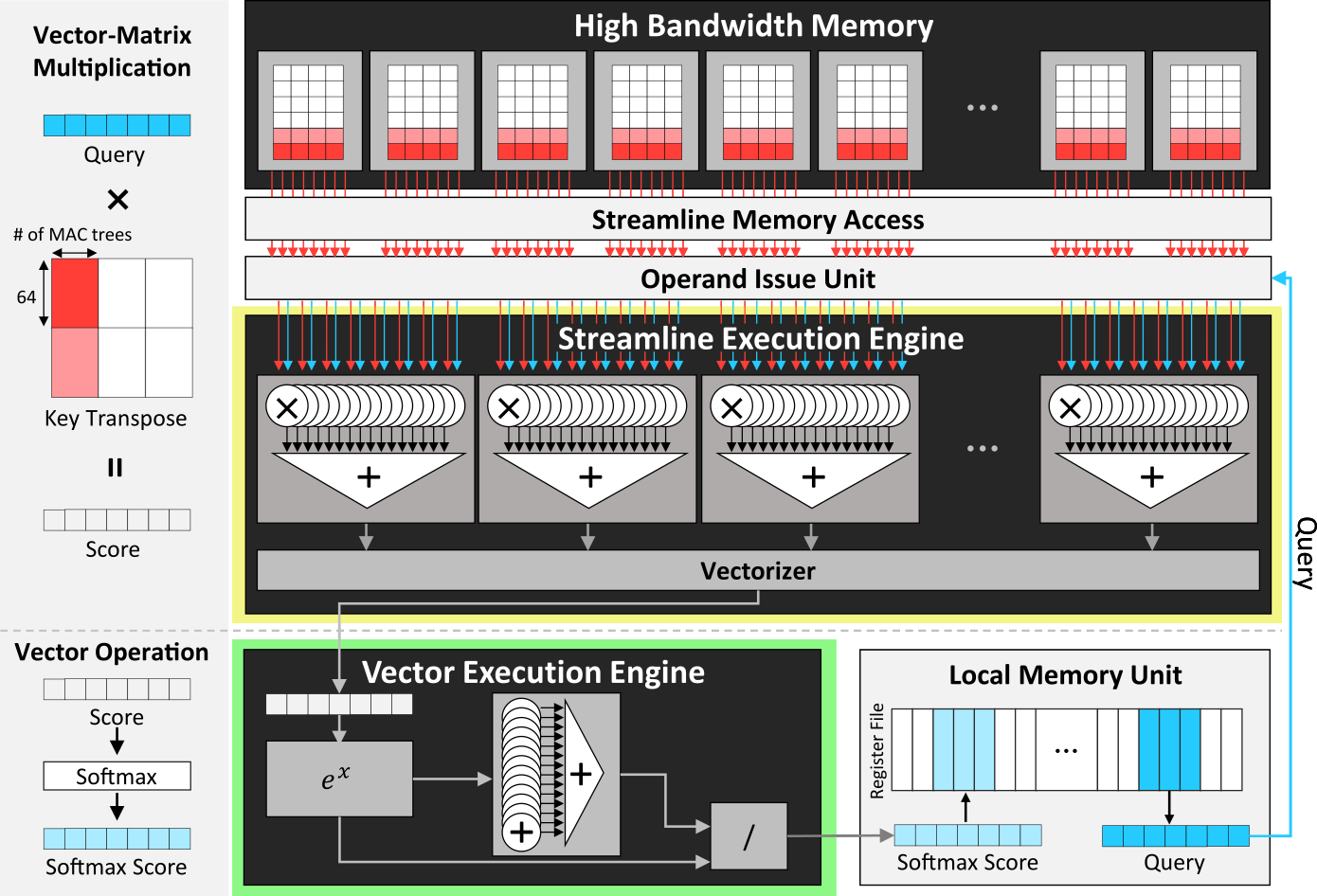
To improve utilization, the LPU architecture scales the MAC units to match the incoming bandwidth. The local memory unit has separate read and write ports to simultaneously supply operands and accept results. To accommodate operations that require transposed matrices, the LPU transposes data on the fly, further streamlining processing. For large models that span multiple LPUs, the architecture divides functions into small tasks that generate output at a rate matching the inter-LPU bandwidth. Pipelining computation and communication, the LPU raises utilization by enabling a processing task to proceed while the previous one transfers results.
The vector unit handles embeddings, performs activation functions, and selects output tokens. In its initial implementation, the vector unit is 64 elements wide because most embeddings are a multiple of 64.
LPU Programming and System Design
Although multiple execution engines comprise an LPU, it’s a unitary processing unit. To coordinate the engines, the LPU includes a RISC instruction control processor, which fetches and dispatches LPU instructions. The LPU instruction set is simple and includes operations for memory access, computing, networking, and control. Additionally, to manage data flow from memory and the register file, the LPU has an operand issue unit. It also configures execution engines.
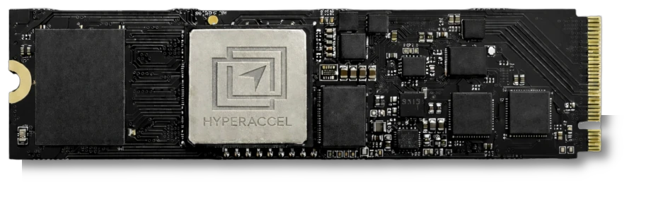
To scale up, a system can contain multiple chips connected by direct chip-to-chip links running a proprietary protocol. The Hot Chips poster describes 8- and 16-LPU systems based on AMD Alveo FPGA cards. For the Bertha 100 and 500, HyperAccel will retain the card-based approach. As Figure 2 shows, the B100 will come on an M.2 module suited to embedded applications, and the B500 will reside on a double-wide PCIe card requiring 250 W. HyperAccel promises the B500 will double the token rate of the two-generation-old Nvidia H100. More importantly, the bigger Bertha has 12 × the power efficiency of the H100, which should make it competitive with the upcoming Nvidia Rubin.
Bottom Line
Most AI accelerators employ systolic arrays for some processing. By extending the data-flow principles of these arrays to the entire chip, HyperAccel expects to achieve superior function-unit and memory-bandwidth utilization. This, in turn, enables its chips to generate LLM tokens using less hardware, slashing power requirements and thereby lowering customers’ operating costs. The company doesn’t provide latency figures, but Bertha should have advantages here, too, positioning it to support interactive chatbots. HyperAccel’s value proposition is clear, but unfortunately for the company, competitors—including Nvidia—are working to address the same challenges.