

AMD has aligned its data-center GPU architecture with that of market leader Nvidia. However, AMD highlights the token-throughput and efficiency gains of the new MI455X over the previous-generation MI355X instead of touting how customers will find it easier to port their AI models to the GPU. Implementing the CDNA 5 architecture, the MI455X is the heart of the Helios-400 platform and will ship to customers later this quarter.
When executing DeepSeek V4 Flash, the new chip is 4–34× faster than its predecessor, with the high end of the range corresponding to higher per-user token rates. At the same time, the MI455X reduces token cost relative to the MI355X, yielding peak savings of 18×. These improvements stem from the increased computational, I/O, and memory resources of the MI455X, as well as numerous architecture changes. The updated chip better positions AMD to compete with Nvidia, delivering a similar architecture and comparable performance, thereby reducing developers’ switching barriers.
CDNA 5 Aligns AMD MI455X with Rival Architecture
The MI455X implements the new AMD CDNA 5 architecture, modifying CDNA 4 and adding features to raise performance. In some cases, AMD drew inspiration from Nvidia.
- Workgroup processors (WGPs) are a construct that CDNA 5 borrows from the AMD RDNA line of PC GPUs. Each WGP pairs two compute units (CUs) and shares local memory (LDS), cache, instruction schedulers, and data-movement hardware. Thus, a workgroup (a group of threads) has access to more resources when mapped to a WGP than when mapped to a single CU in CDNA 4, the MI355X architecture. A WGP corresponds to a streaming multiprocessor (SM) in the Nvidia architecture.
- Compute units underwent an overhaul in CDNA 5. Previously, a CU handled 64 threads—a wavefront—at a time (Wave 64). However, the MI355X broke the wavefront into four chunks, issuing 16 at a time to a 16-ALU SIMD unit and requiring four cycles to process all 64. The new architecture reduces wavefronts to 32 threads and doubles the number of ALUs per SIMD unit to 32 (Wave 32). Thus, a CDNA 5 CU can issue a new wavefront every cycle. The finer granularity should raise utilization. Importantly, the 32-thread wavefront is consistent with Nvidia’s conceptually similar 32-thread warp.
- Transcendental support improves with CDNA 5. As before, inside a CU alongside a SIMD (vector) unit lies a transcendental unit. The latter now supports tanh, a transcendental function often used by neural-network activations. Without this support, computing the function entailed vector operations, occupying SIMD hardware and taking more cycles. Adding tanh brings the AMD GPU in line with the Nvidia offering.
- A tensor data mover and a multicast engine streamline data movement in CDNA 5. Instead of tying up CU resources to coordinate exchanges of tensor data between CU local memory and DRAM as before, the new tensor data mover handles the transfers, enabling simultaneous data movement and computation. This data mover is similar to the Nvidia tensor memory accelerator (TMA). The AMD multicast engine and the Nvidia TMA multicast function address the case where multiple WGPs/SMs require copies of the same data.
- FP4, FP6, and FP8 data types receive expanded support. For example, the scaling factor in the MXFP4 format can apply to a 16-element block instead of only a 32-element block, and the scaling factor can be fractional. Effectively adding precision, these changes should improve the accuracy of quantized models. Here, too, the changes align with the Nvidia approach.
- Structured sparsity is supported in hardware and, therefore, is more likely to be tapped by developers. Pioneered for data-center use by Nvidia, structured sparsity zeroes out two of every four matrix values, reducing memory consumption and increasing throughput by allowing hardware to skip multiplications involving these zero factors.
MI455X Memory Hierarchy
The MI455X memory hierarchy differs from that of the MI355X, generally increasing capacity and bandwidth.
- Register-file size remains at 128 kB per wavefront in the CDNA 5 architecture. Although this matches the size of the MI355X register file, it actually doubles the per-wave capacity because the Wave 32 CDNA 5 shares this capacity among half as many threads as the previous-generation architecture.
- Local storage increases, with each CDNA 5 WGP providing 384 kB shared between two Wave 32 CUs compared with 160 kB per CDNA 4 Wave 64 CU.
- The cache hierarchy undergoes a redesign, eliminating some layers and altering the capacity of others. The MI455X eliminates the 32 kB L1 cache within the CU and the 256 MB Infinity Cache (last-level cache). In place of a 4 MB L2 cache per compute die, the MI455X has a 96 MB L2 cache shared among four compute dice, increasing data reuse. The new approach reduces memory transactions traversing major boundaries, decreasing power and latency because the L2 can service requests that previously would’ve gone to the Infinity Cache. Moreover, the bandwidth between the compute dice and L2 cache is 1.5× greater than the bandwidth to the Infinity Cache in the old design.
- HBM capacity doubles to 432 GB, and bandwidth is 2.9× greater, following an upgrade from HBM3E to HBM4.
- DMA is topology aware in the MI455X. DMA engines process requests and balance transactions that span chips among scale-up links.
Comparing AMD MI455X, AMD MI355X, and Nvidia Rubin
In terms of key product attributes, the MI455X GPU is 1.5× to 4× as powerful as the MI355X and, other than HBM capacity, is similar to the Nvidia Rubin GPU, as Table 1 shows.
|
|
AMD MI455X |
AMD MI355X |
Nvidia Rubin |
|---|---|---|---|
|
FP4 Throughput |
40.26 PFLOPS |
10.1 PFLOPS |
50 PFLOPS |
|
HBM Capacity |
432 GB HBM4 |
288 GB HBM3E |
288 GB HBM4 |
|
HBM Bandwidth |
23.3 TB/s |
8.0 TB/s |
22 TB/s |
|
Bidirectional Scale-Up BW |
3.6 TB/s |
1.07 TB/s |
3.6 TB/s |
Table 1. Comparing the AMD MI455X with the MI355X and Nvidia Rubin, the new AMD GPU hikes computational and data throughput over its predecessor and promises performance similar to its rival. (Source: vendors.)
MI455X Chiplets and Interconnects
The MI455X comprises multiple chiplets, as Figure 1 shows.
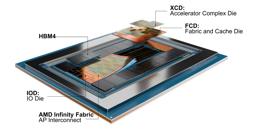
- 8× XCD—eight 2 nm accelerator complex dice (XCD), referred to above as compute dice, each containing two shader engines made of 16 WGPs and their shared resources plus two redundant WGPs.
- 2× FCD—AMD organizes the XCD in groups of four, bonding each to a fabric and cache die (FCD). Fabricated in the TSMC N3P process, each of the two FCD interfaces with six HBM4 stacks, interconnects the four XCD, and implements the 96 MB L2 cache.
- 2× IOD—two I/O dice (IOD) link the MI455X to other chips, together providing 3.6 TB/s across 72 UALink-over-Ethernet (UALoE) lanes to scale up, 256 GB/s of AMD’s proprietary Infinity Fabric (also called xGMI) bandwidth for connecting an AMD Epyc (Venice) host, and additional PCIe Gen 6 or UALink ports for attaching network interfaces. In addition to retaining Infinity Fabric to connect the host CPU, AMD also employs the protocol within the MI455X. However, for GPU-GPU scale-up connections, AMD has replaced Infinity Fabric with UALoE, enabling a 72-GPU scale-up domain like Nvidia Rubin achieves using NVLink.
- 12× HBM stacks provide 432 GB of total capacity.
Bottom Line
The MI455X differs significantly from the MI355X and previous AI-targeted Instinct MI300 GPUs. The new chip boosts computational throughput, memory capacity, and bandwidth as expected. It also updates caching and data-movement approaches, reflecting how real-world performance depends on efficiently shuttling data. Smaller changes, such as implementing tanh, will further raise throughput, even though they don’t affect peak throughput or bandwidth. Many of the changes align AMD’s architecture with Nvidia’s, which should facilitate customers’ MI455X adoption.