Four years after disclosing its D1 AI accelerator (NPU), the heart of its Dojo system, electric-car company Tesla has pulled the plug. After unveiling the D1, the company touted grand plans, promising in July 2023, when it began Dojo production (a year after the initial public target), that it will have deployed enough computing capacity by the start of 2024 to be a Top 5 supercomputer operator and will have a more powerful Dojo V2. When V2 chips finally entered production a month ago, the company began promising a V3. Both new versions are now canceled, and V1 deployments have been small. Tesla’s plan is to somehow build another data-center system using its upcoming AI6 inference chips.
Unusual Engineering Approaches
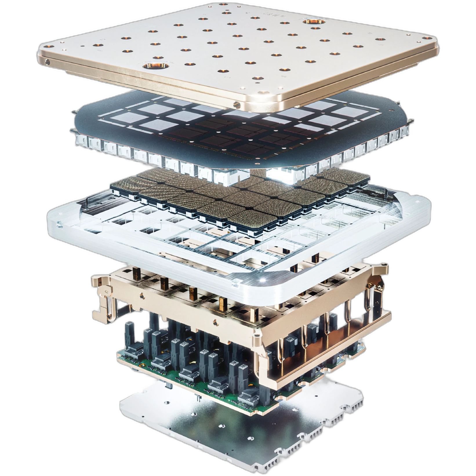
Kludges, hacks, and groundbreaking engineering can be nearly indistinguishable, and it’s difficult to know what category applies to the Tesla Dojo. The company built a 15 kW tile about 8 inches (200 mm) across that contained 25 of its custom D1 accelerators, reaping some of the benefits of Cerebras’s wafer-scale integration—and facing similar I/O and memory-interface constraints. To mitigate these issues, the company built another custom chip and put it on boards hung from Dojo’s six-tile trays—kludge, hack, or groundbreaking engineering?
Acknowledging Long Odds
In its January 2024 earnings call, Tesla CEO Elon Musk admitted that Dojo was a long shot and that it would keep acquiring Nvidia GPUs (many of which it transferred to its corporate sibling XAI). Even in the timeframe that it said it would be ramping production, the company was confessing it had overpromised.
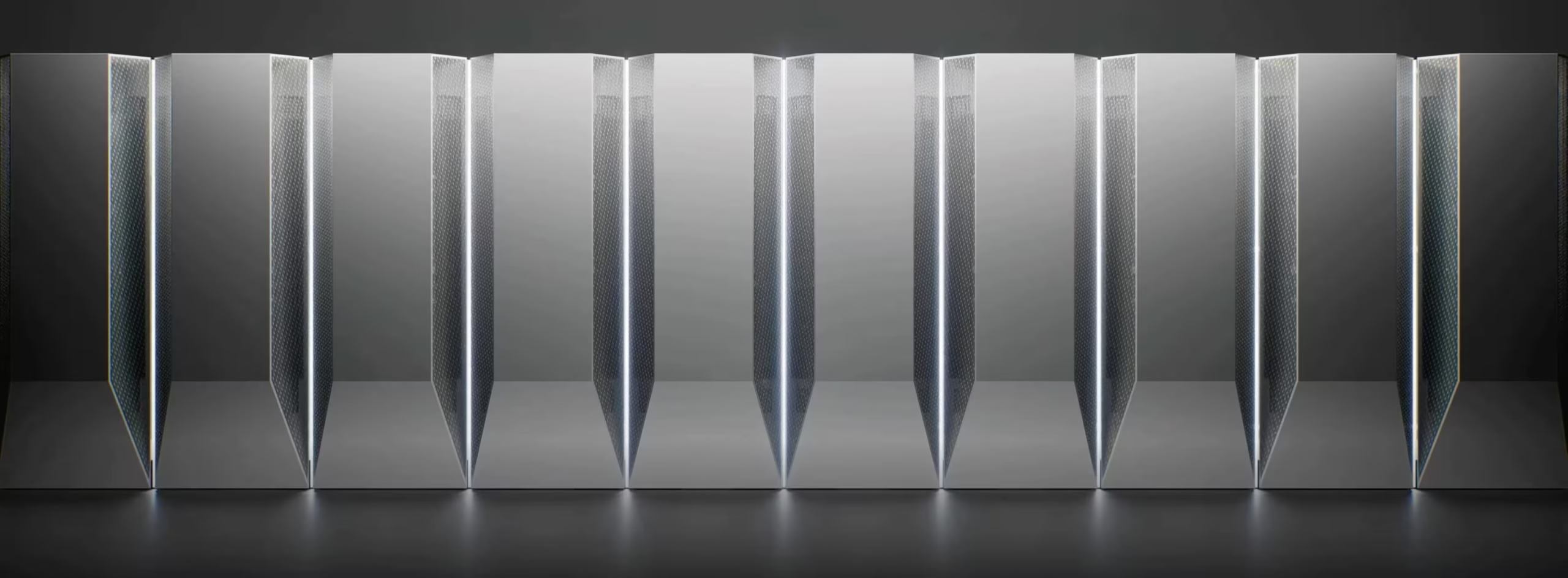
The company bit off a lot. In addition to its groundbreaking semiconductor packaging (the tile), the D1 employed 354 copies per die of a proprietary CPU. An “exapod” (Dojo system) comprises multiple cabinets containing multiple trays, each holding six tiles, yielding 1.1 EFLOPS. In addition to stylish good looks (see Figure 1), power requirements were so high that, when turning on a prototype, Tesla blew a circuit breaker—for the city.
Chips and DIPs
The second custom chip, the Dojo Interface Processor (DIP), addressed I/O and memory-interface bandwidth. It was another big design, and 20 two-DIP cards attach to each tray. The DIPs bridged the D1 to HBM—the NPU lacked memory interfaces—and Ethernet ports provided an additional connectivity layer beyond a tray’s primary X-Y mesh. In addition to custom hardware, Tesla developed a proprietary transport protocol for the network, the Tesla Transport Protocol over Ethernet (TTPoE). The added Ethernet interfaces and TTPoE enabled a D1 to communicate directly with a far node, not just an adjacent chip.
The DIPS, with their HBM and added networking, solved a critical problem. An earlier Dojo revision didn’t include them, but Tesla found the D1s were data starved. Their utilization was only 4%. DIPS rectified this without forcing the D1 to be redesigned.
Bottom Line
A Dojo V2, or at least a V3, would presumably have been a cleaner design. Those newer systems could’ve been more conventional. If Tesla had limited the application scope to training driver-assistance systems, the company could’ve simplified its design and achieved greater throughput per watt and per dollar than by employing off-the-shelf GPUs. Its ambitions were always greater, however, targeting humanoid robots and other AI applications. Breakthroughs often come from unreasonable expectations, but delays and failures are more likely.