
Intel has trickled out additional information about its forthcoming Core Ultra 3 and Xeon 6+ PC and server processors. Better known as Panther Lake and Clearwater Forest, they’re Intel’s first 18A products. Amid reports that the 18A process has suffered poor yields, the company seeks to mitigate concerns by showing off the new chips and its Arizona fab. The new processors also encourage rethinking the company’s E-core prospects.
Intel 18A Recap: GAA and Backside Power
Taking its name from its nominal 18 angstrom (1.8 nm) critical dimension, Intel 18A incorporates two new technologies:
- Gate-all-around (GAA) transistors
- Backside power
This is Intel’s first process to employ GAA, which it calls Ribbon FET. The successor to FinFETs, a GAA transistor provides finer-grained control of current and reduces leakage. The technology also raises transistor density and lays the groundwork for future complementary FETs, which stack transistors on top of each other. TSMC will introduce GAA technology with its contemporaneous N2 (nominally 2 nm) process. Samsung started using it in the 3 nm generation.
Intel is the first company to commercialize backside power, which the company calls Power Via. Chips previously routed power and ground at the top of the metal stack, requiring vias to drop past many metal layers to reach transistors. Backside power, however, routes Vdd and ground on the back of the die and tunnels them up and around to the front to contact the transistors. This approach reduces IR drop on the power rails and improves chip density.
Clearwater Forest Configuration Highlights
Intel revealed two differences between Clearwater’s chiplets (tiles) and those in past chiplet-based Xeons:
- An active base tile
- Many (12) computing tiles
Active Base Tile
The active base is unusual. Multi-die designs have employed passive silicon base tiles containing only wiring to connect adjacent chiplets, but active bases are unusual. Intel employed one in its Ponte Vecchio data-center GPU, disclosed in 2021. That tile integrated PCIe interfaces and cache. Clearwater Forest puts DRAM controllers and cache in its three base tiles and employs separate tiles for I/O and the silicon bridges (EMIB) that connect adjacent chiplets.
Because SRAM doesn’t scale as well as logic with each new and ever-more-expensive process node, putting cache in a separate, older-technology chiplet can reduce cost. For Clearwater, Intel makes the base using the Intel 3 process. Employing multiple base tiles enables the company to configure SKUs with different cache capacities and DRAM bandwidths.
Computing Tiles
Clearwater’s only Intel 18A components are its computing tiles. Whereas recent chiplet-based Xeons have had a few large computing tiles, Clearwater has 12, each containing 24 Darkmont E-core CPUs. (An E-core is a CPU that deemphasizes performance to achieve better power and area efficiency, in contrast to a performance-optimized P-core.) By employing more, smaller dice, Intel achieves a higher yield for a given defect density. This improves Clearwater’s manufacturing costs, a risk mitigation for a product relying on a process node that has struggled to yield acceptably.
Panther Lake Configuration Highlights
Although Intel’s manufacturing problems have garnered more attention over the past ten years, its PC processors, meanwhile, ceased to be well ahead of its competitors technologically. A few generations ago, the company adopted a hybrid-core approach that integrates P- and E-cores. The latter helped Intel post strong scores on multicore benchmarks but delivered little practical value. When the company introduced its most recent thin-and-light laptop processor, Lunar Lake, it began to show how E-cores could reduce power, finally demonstrating value.
Panther offers more power-management capabilities. Like Meteor Lake, Lunar’s predecessor, it integrates three CPU tiers: P-cores, E-cores, and low-power E-cores (LPE cores). Panther puts the E-cores on the main processor bus, eliminating a bottleneck throttling their performance. The LPE cores, which have had little utility, except in Lunar, raise L2 cache capacity, helping them to stay fed with data and instructions. Panther also adds a system (memory-side) cache, which the LPE cores can access. Intel’s Thread Director software, which hints to the OS how to assign processes to CPUs, has also improved.
The E- and LPE cores implement the Darkmont microarchitecture, discussed below. Darkmont enhances Arrow Lake’s Skymont. (Arrow targets midrange and high-performance laptops and desktops.). Panther’s E-cores are like those in Clearwater. The P-cores implement the Cougar Cove microarchitecture found in Arrow Lake and Granite Rapids Xeons. The updated CPUs, new SoC capabilities, and 18A process enable Panther to deliver performance on par with Arrow Lake but with the lower power of Lunar Lake.
Panther also integrates an NPU upgraded from that in Lunar and Arrow. Raw performance measured in TOPS is about the same but area efficiency and real-world throughput increase. The new NPU also adds support for eight-bit floating point (FP8).
Like Meteor, Lunar, and Arrow, Panther is a chiplet-based design using a passive silicon substrate. Panther has a computing tile fabricated in the 18A process, an I/O tile (platform controller) made by TSMC, and a choice of high-performance and low-cost GPU tiles fabricated in Intel 3 or TSMC N3E. Lower-priced SKUs can disable the computing tile’s 8 E-cores. As with Clearwater, reducing the computing tile’s scope improves its manufacturability. A further advantage of the chiplet approach is the option to reduce costs by using the smaller GPU option.
Darkmont
Intel’s E-cores have proven problematic. In server processors, they enable higher core counts and help Intel compete with Arm-based designs but (like merchant-market Arm server chips) haven’t proven popular. Performance has been too compromised. For PC processors, as noted above, they’ve done little beyond pumping up benchmark scores. We have seen the all-E-core PC processor on the horizon as a disaster in the making, providing multicore throughput but not the single-thread performance that applications require.
However, Darkmont invites reassessing E-cores. It and Skymont are smaller than Intel’s P-cores but aren’t weak. Execution width is similar to the most powerful Arm- and RISC-V-compatible CPUs, such as the Qualcomm Oryon-L and the Tenstorrent Ascalon. The front end is effectively eight wide, and the badonkadonk is huge. It offers 26 execution ports and provides eight integer ALUs and four SIMD/FPU pipelines, as Figure 1 shows. The lattermost are twice as many as Skymont and now include support for VNNI instructions to raise AI-workload throughput. However, to conserve area, we expect Darkmont’s branch prediction to be less extensive than that of Intel’s P-cores and competitors’ high-performance CPUs.
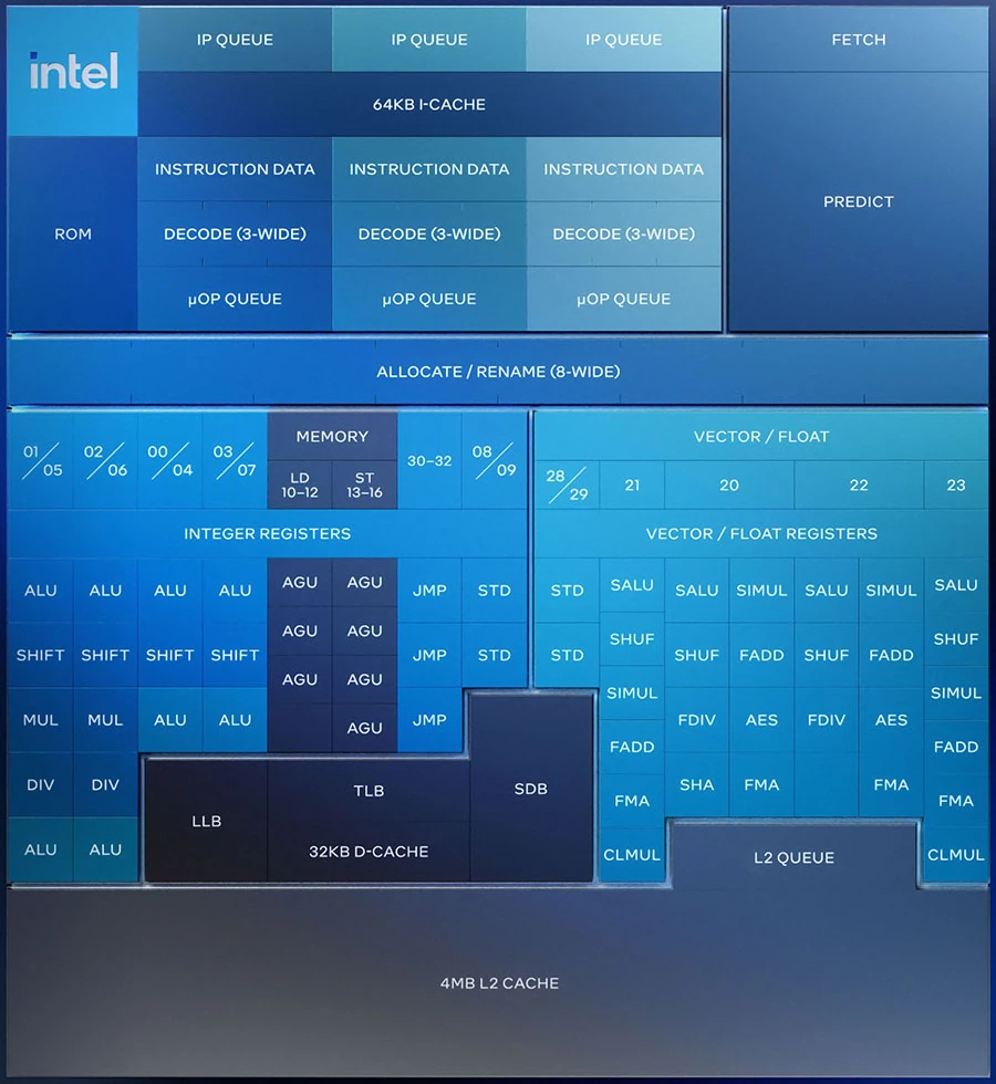
Those cores also have eight or more decoders, a major die-area consumer. Darkmont has nine decoders in total, but they’re implemented as three groups of three. A challenge with decoding an x86 instruction is that its size can’t always be determined before decoding begins. Thus, the starting point for subsequent instructions can’t be determined, either. Couger Cove’s eight-wide decoder must consequently have extensive logic to look ahead and identify instruction boundaries.
Darkmont’s three-wide decoders need less of this logic. However, the three blocks must work on nonconsecutive code, such as the current instruction block and two speculative branch targets. Thus, they’re not as effective as other CPUs’ eight-plus decoders. (AMD’s Zen 5 CPU has two four-wide decoder blocks, each dedicated to one of the CPU’s two threads.) Cougar Cove, moreover, has a Level 0 micro-op cache that can send 12 operations to the back end per cycle, further enhancing its front-end throughput.
Bottom Line
E-Cores
Intel states that a 288-core Clearwater processor will deliver 17% better throughput than a same-size Sierra Forest, which used Skymont’s predecessor, Crestmont. It’s not a great gain for a two-generation-newer CPU, and we still harbor doubts about E-core server chips and hybrid PC processors. However, we see a path toward future E-cores that raise instruction throughput (IPC) to a competitive level but still deliver better power and area efficiency than Intel’s P-cores.
18A
We noted that Intel could come out ahead if it plowed forward with 18A chips even if yields lagged targets. Production enables the company to examine where defects and other problems occur and heightens the incentive to rectify them. By the time Panther approaches the middle of its lifecycle, yields could be on target. If they aren’t, Intel has mitigated risk by committing only Panther and Clearwater to the process, contracting with TSMC for its main PC and server processors, Nova Lake and Diamond Rapids.
Equally, this reliance on TSMC undermines the key message of Intel’s recent promotional effort. If 18A is doing great, why doesn’t Intel entirely trust it for its own products? An 18A-based midlife kicker for Nova and Diamond or other commitment to the process would be more persuasive than a few additional details about long-disclosed chips and a fab tour.