Google has unveiled its eighth-generation AI accelerator, revealing a design similar to past designs but with greater per-socket throughput, faster networking, and new collective engines. Per-chip gains should improve cost per token and performance, particularly as large language models grow well beyond 1 trillion parameters. As with some previous generations, the new accelerator (NPU) has separate implementations for training and inference (TPUv8t and TPUv8i). They will be generally available by the end of the year.
What’s New in Google TPUv8: Architecture and Specifications?
- One-year cadence—Google disclosed TPUv7x (Ironwood) only a year ago and is revealing the TPUv8 architecture in advance of availability. By contrast, three years separated TPUv3 and TPUv4, with technical disclosure deferred until the end of their lifecycles. This cadence and early disclosure indicate the company remains keen to have an alternative to merchant chips and to meet the needs of external customers, such as Anthropic and Meta. The virtualized instances that Google offers cloud customers are likely less important because they don’t sum up to the massive hardware demand of an AI company or hyperscaler.
- Scale-up bandwidth doubles to 19.2 Tbps per chip for both TPUv8 versions compared with the TPUv7x (Ironwood).
- Inference pod size has grown 4.5× to 1,152 TPUs. We expect this larger scale-up domain will speed up large models by enabling Google to dedicate a chip to a specific part of the neural network.
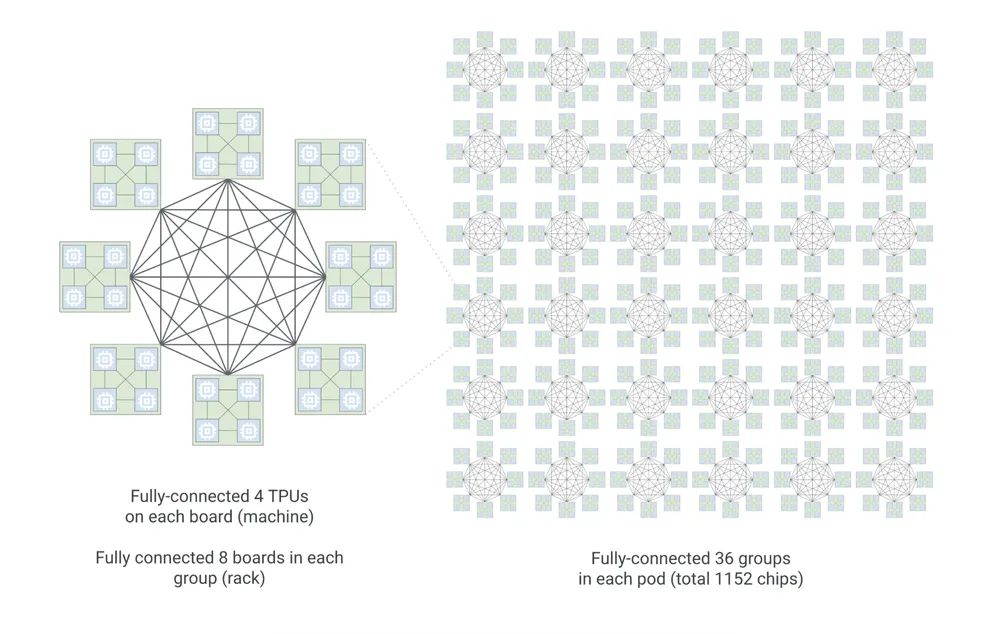
- Inference pod topology has changed to a layout Google calls “boardfly.” Figure 1 shows how boardfly fully interconnects 36 groups (racks) of TPUs. Each group comprises eight fully interconnected boards. Each board contains four fully interconnected chips. Previous-generation inference-only pods’ topologies didn’t scale up as far; see the company’s visualization. A large low-latency topology should speed up mixture-of-experts (MOE) models, which break models into chunks (experts) that work independently in parallel before sending results to a central node to be coalesced.
- The training scale-out network now implements Google’s Virgo network technology, which enables 134,000-TPU clusters. Delivering four times the bandwidth (400 Gbps) per TPU, the new network should accelerate training, which can spend 30% of run time transferring data. The torus/hypercube training topology is nearly unchanged from previous generations but now supports slightly more nodes.
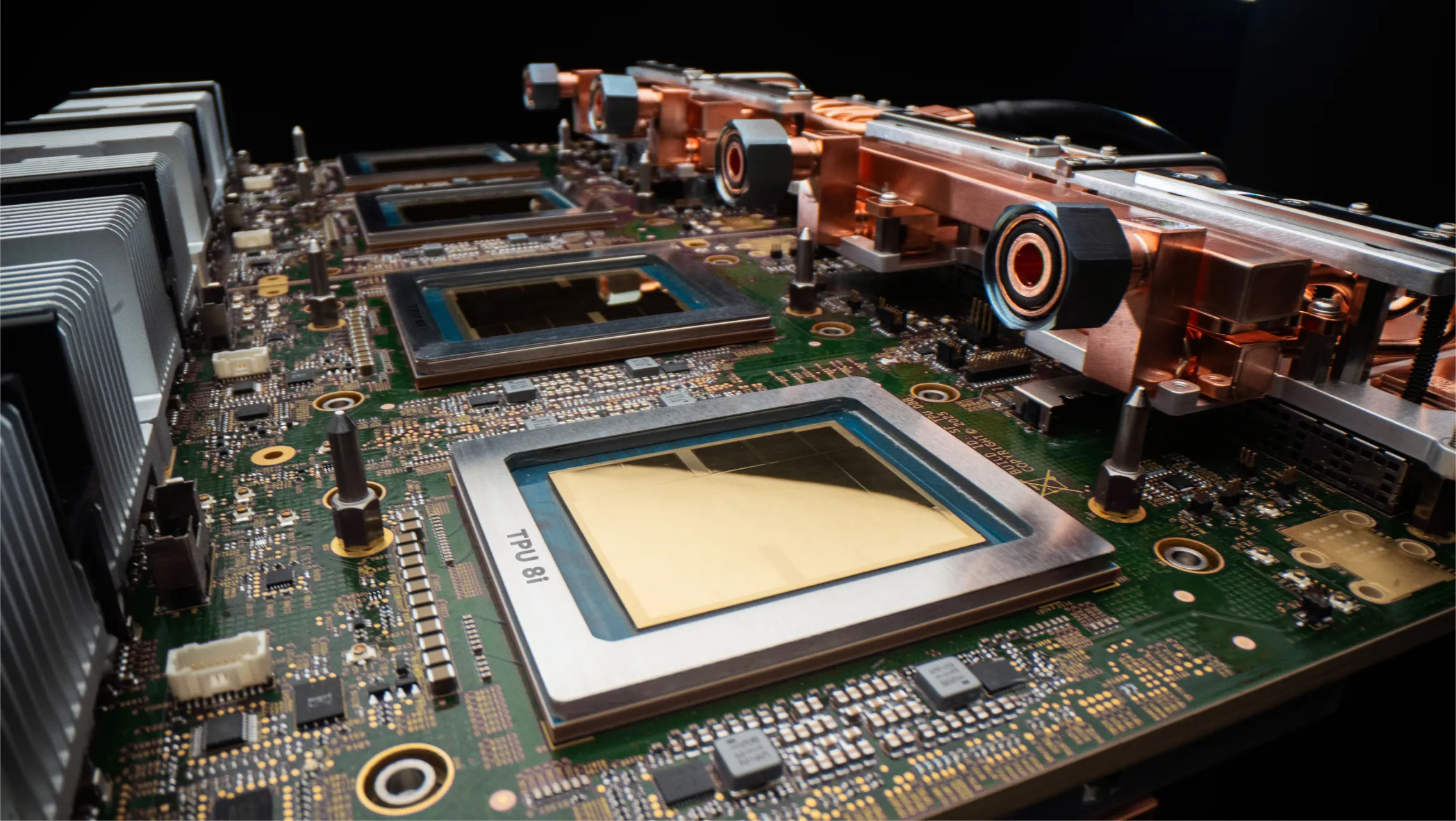
- On-chip SRAM (vector memory or VMEM in Google’s vernacular) triples to 384 MB in the inference chip compared with Ironwood, larger KV caches and greater context lengths in large language models (LLMs). The company withheld the training-focused TPUv8t’s VMEM capacity.
- Training FLOPS increase over the previous-generation TPU, but the details are murky. Google cites a 2.7× speedup on FP4 data for training, although that microformat is less commonly employed in training than inference. The company has withheld performance scaling for other data types. Many NPUs halve throughput as word size doubles. (Alternatively, they double throughput as word size halves.) However, TPUv7x didn’t have a four-bit execution path; therefore, FP4 operations ran at the same rate as FP8. Without further details, we cannot assess throughput increases for 8-and 16-bit formats. Generational gains are required for the TPUv8 to rival the raw throughput of Nvidia Rubin.
- Inference FLOPS more than double from the TPUv7x. On the basis of Google’s pod-scale FP8 rating, we infer per-chip peak performance to be 10 PFLOPs. As above, we require information on other formats—particularly FP4 for inference—before drawing conclusions.
- The Arm-based Google Axion processor (CPU) provides general-purpose computing resources, compared with the x86 processors Google has used. The company withheld whether it employs a proprietary chip-to-chip interconnect between CPUs and TPUs, suggesting that it still relies on PCIe. In the past, Google employed one host processor per four TPUs, which maps to boardfly’s four-TPU boards and one hypercube face in a training system. A proprietary interface, like Nvidia uses, could improve system throughput.
- Collective engines are a new TPU-architecture feature. Google indicates they can reduce latency by 5× but hasn’t elucidated how or stated an overall performance improvement. As alluded to above, MOE employs more scatter-gather and other collective operations, motivating the new offload engines. Moreover, any LLM at data-center scale relies on collectives, and overlapping data movement and associated operations with computing can raise performance and reduce costs. Originally added to address HPC applications, Nvidia has long implemented collective acceleration. It’s unclear how commonly customers employ Nvidia’s technology, but Google’s prime customers are internal groups and better positioned to harness such engines than typical developers.
Bottom Line: Is Google’s TPUv8 Better Than Nvidia Rubin?
Because internal use dominates the TPU business case even as Google seeks outside customers, comparing TPUs and GPUs requires looking at more than raw throughput. Google retains its advantage in scaling up AI systems. Even as Nvidia considers rack- and cluster-level scaling more than before, it still addresses small-scale (e.g., eight-GPU) systems, whereas Google deploys training TPUs only in big pods. For inference, Google must only support a few production workloads, whereas Nvidia must support many and win diverse customers. The GPU maker, therefore, invests heavily in software.
Nvidia dominates MLPerf benchmarks, revealing that, in addition to high-performance silicon suitable for diverse deployments, it has the resources to tune models and software. We expect the TPUv8 to be less costly for Google to deploy and operate than the Nvidia Rubin. Real-world performance must be similar, but even raw-throughput details are still scarce. Google has submitted MLPerf results in the past, and TPUv8 data would reveal exactly how competitive it is. For the company to cement itself as a merchant-market alternative to Nvidia, it must be clear about the performance and cost advantages TPUv8 delivers.