
The x86 Ecosystem Advisory Group (EAG, better known as AMD and Intel) has defined the AI Compute Extensions (ACE) for the x86 architecture. The group frames these instructions as a palette, a term Intel coined for a specific configuration of its Advanced Matrix Extensions (AMX). Those AI-focused instructions and associated hardware first appeared in Sapphire Rapids Xeons.
As AI functions have become increasingly used, CPU vendors have sought to accelerate them without requiring software to call a separate chip. Matrix multiplication, which neural networks rely on, is a prime target for CPUs to speed up. Adding a multiplier array to a core, however, requires substantial die area, increasing chip cost. An Intel AMX unit occupies 12% of total CPU area (including the L1 cache and a 1.25 MB L2 cache). About a quarter of that area is for matrix-register tiles. The rest is for the multiplier arrays.
Adding AI Instructions With Minimal Die Area Growth
ACE addresses this cost by focusing on outer-product operations. These use AVX SIMD registers as input, structuring a 512-bit register as an n × 4 input matrix, where n is 512 divided by 4 times the word size. For eight-bit data, each SIMD register holds a 16 × 4 matrix. ACE computes the n four-element dot products of the inputs and stores each result in a cell of the AMX-defined matrix-register tiles, as Figure 1 shows.
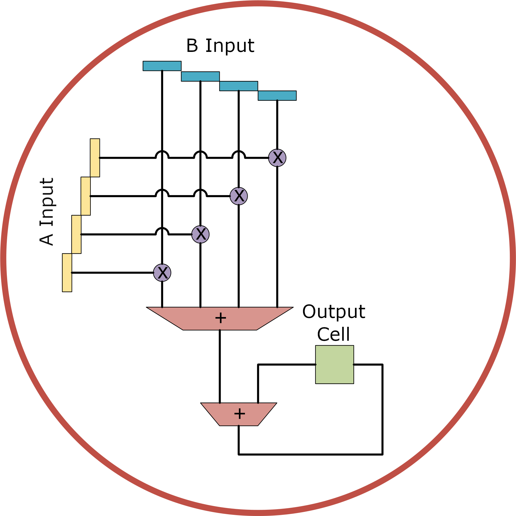
While a single ACE instruction computes all cells in the output tile, the ACE spec doesn’t stipulate that hardware implements an array of multiply-accumulate units (MACs) or only enough MACs to compute a row at a time. The latter requires the same number of MACs as needed to support the AVX dot-product instruction, conserving die area (particularly if an ACE implementation reuses the AVX MACs).
Little added performance would come from implementing a large multiplier array. ACE has no instructions using matrices as source operands—not even loads or stores. Thus, using the results of an outer-product operation requires code to transfer data one row at a time from the destination matrix to an AVX vector register. Filling the tile faster doesn’t speed up matrix operations because it takes so long to write results to memory. A similar speedup is possible by overlapping transfers with row-by-row computation using only the extant AVX hardware. Therefore, while ACE should increase die area by only 3%, AI models will speed up only modestly.
ACE Is the First to Define FP4 CPU Instructions
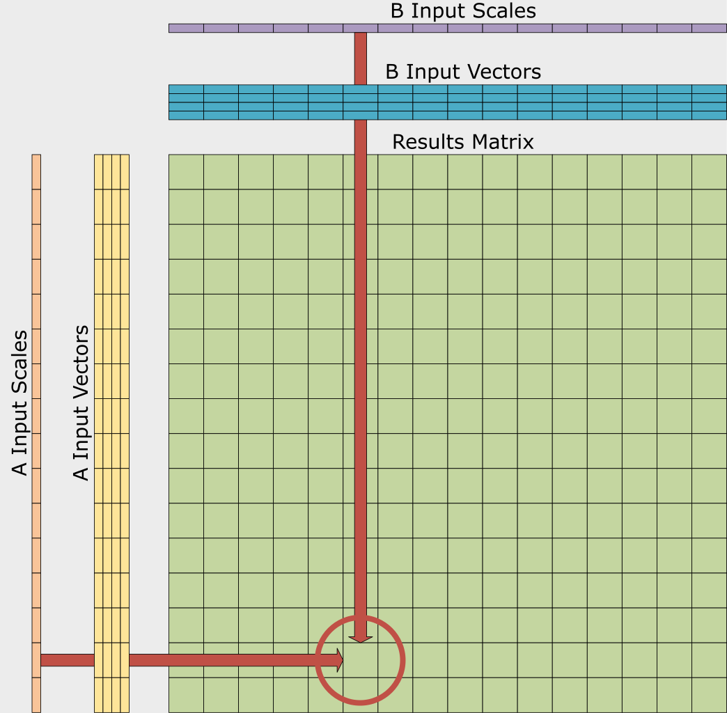
ACE also adds support for FP4. It and similar formats combine low-precision values with a scaling factor. ACE defines registers to hold the scaling factors corresponding to 16 low-precision values. Hardware can apply the factors during outer-product operations, as Figure 2 shows. Additionally, ACE includes instructions for converting between formats.
Bottom Line
In summary, AMD and Intel have agreed to instruction-set extensions in advance of implementing them, cooperation that contrasts with previous x86 developments led first by one company and subsequently copied (or ignored) by the other. ACE should accelerate AI operations, particularly those on low-precision block formats like FP4. Importantly, ACE should raise CPU complexity and area only slightly.
However, ACE offers less capability than corresponding extensions for Arm and IBM Power architectures. Arm and IBM balanced capability and die area by sharing matrix hardware among multiple CPU cores. This is a superior approach. Matrix units are unlikely to be heavily utilized by multiple threads simultaneously. When they are used, developers will want much more throughput than ACE can provide.
A further complication is that no killer AI-enabled app for Windows PCs has emerged. The AI PC concept has so far flopped. When one does emerge, the x86 and Arm camps must clarify for developers the cases better matched to the CPU instead of the more powerful local NPU. The same need for clarity applies to servers. There, Arm is quickly eroding x86 share, a trend that half measures for better CPU-based AI computation will do little to staunch.