Tamping down speculation about the viability of its MTIA AI accelerator, Meta has disclosed its roadmap for the NPU family. The company is speeding up the pace at which it introduces new versions, revealing plans to deploy three designs this year and next after recently deploying its third-generation MTIA300.
We believe the first MTIA (now called the MTIA 100), which the company began in 2020, served only as a development vehicle, while the second-gen MTIA 200 (FKA the MTIA 2i) had limited deployment. Thus, we have been skeptical of the MTIA project, especially because Meta recently struck deals to source GPUs from AMD and Nvidia, as The Byrne-Wheeler Report (BWR) recently covered. But, as the same BWR episode discussed, Broadcom has indicated that MTIA production was set to ramp.
Meta initiated the MTIA project the same year that Nvidia began producing the A100 GPU. The social media company was running ranking and recommendation models (we’ll conflate these concepts) to serve up engaging Facebook posts and, more importantly, advertisements. These models combine processing embeddings and fully interconnected neural-network layers, the same sort of pairing that large language models (LLMs) had begun to use. In 2020, whether and how to offload recommender execution from CPUs was unsettled.
MTIA 200 Improves the MTIA 100 Architecture
Meta compared the MTIA 100 with an Nvidia GPU and the Intel NNPI, a design the chipmaker obtained through its Nervana acquisition. The first-gen MTIA outperformed the NNPI and rivaled the GPU. (Intel subsequently called a mulligan on Nervana and acquired Habana, which it then killed to focus on data-center GPUs.) Meta later A/B tested the MTIA 200 against Nvidia GPUs by running live production workloads on both.
The MTIA 200 refined Meta’s architecture, tripled raw INT8 throughput to 358 TOPS, doubled the on-chip memory to 256 MB, and boosted external memory bandwidth by a third. The company’s goal was for the MTIA 200 to be more cost-effective than GPUs and flexible enough to run more of the company’s production workloads than the first-gen chip. Importantly, it supported PyTorch’s eager mode, enabling neural-network execution without mapping the model to a graph, a feat that some other NPUs couldn’t achieve.
As previously alluded to, the MTIA 100 and 200 had capacious on-chip memory. They also connected to standard external DRAM and did not integrate HBM. The on-chip SRAM enabled MTIA to meet Meta’s latency requirements for recommendation neural networks. (The only thing worse than online ads is having to wait for them.) Moreover, these models are smaller and have more locality than LLMs, obviating HBM. Although they’re optimized for smaller models, Meta found the MTIA 200 outperformed expectations on larger ones as the NPUs tended to be less underutilized as loads varied. These first two MTIA generations supported INT8 and FP16 types. The MTIA 200 added dynamic INT8 quantization, but the company found that feature hard to use.
An MTIA 200 node had a single CPU with six two-NPU modules connected through a PCIe switch. The twelve MTIA 200s formed what today we call a scale-up domain. Two 200 Gbps NICs connected a node to a cluster. A server chassis integrated two such nodes operating independently. Meta’s A/B testing revealed that 24 MTIAs performed similarly to an eight-GPU server but at a lower cost.
The MTIA 300’s Key Technical Upgrades Mark a New Direction
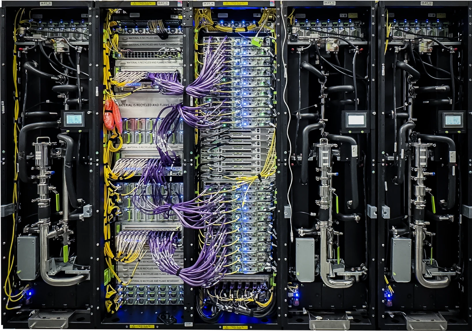
Recently entering production, the MTIA 300 targets recommendation-model inference as its predecessors did, and it can handle training. Its computing architecture is like its forbears. Notably, however, HBM replaces standard off-chip DRAM, as Figure 1 shows. Other changes include:
- FP8 and MX8 (another eight-bit floating-point format) join the list of supported data types. Once the main half-size alternative to FP16, INT8 has fallen out of favor in the data center.
- NICs directly attach to the computing die and reside in the package on two chiplets that integrate six 800 Gbps controllers each.
- The scale-up domain climbs to 16 MTIA chips.
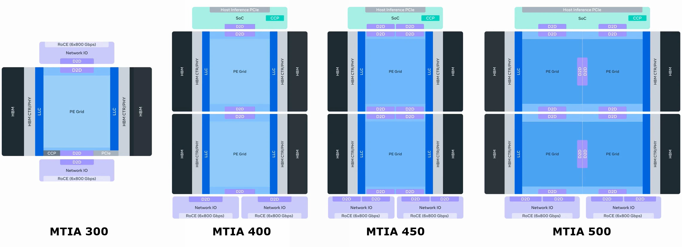
MTIA 400’s Specs Rival Those of Nvidia Blackwell
In Meta’s labs for evaluation in advance of deployment later this year, the MTIA 400 departs further from the original template:
- Target workloads expand beyond recommendation models.
- Two computing dies comprise the chip.
- HBM bandwidth increases by 50% compared with the MTIA 300 and surpasses that of Nvidia Blackwell, and HBM capacity matches that of Blackwell Ultra.
- FP8 (and MX8) peak throughput is 5 × that of the previous generation, topping that of Blackwell.
- The MTIA 400 adds FP4 (MX4) support, and its peak throughput also tops Blackwell’s.
- The PCIe ports and other host-interface functions move to a separate chiplet.
- The scale-up domain climbs to 72 chips, ala Blackwell.
Meta Sets a Timeline for MTIA 450 and MTIA 500 Generative AI NPUs
Scheduled for early 2027, the MTIA 450 targets generative AI workloads and builds on the MTIA 400 with several updates:
- HBM bandwidth doubles.
- Raw FP4 throughput increases by 75%.
- Computing tiles add accelerators for attention layers and the feed-forward network.
- Meta tweaked low-precision floating-point operation, including allowing mixed-precision computation with a discrete conversion step.
The MTIA 500 repartitions computing resources, distributing them among four smaller dies. Due to deploy in late 2027, FLOPS and bandwidth exceed that of the MTIA 450 by as much as the MTIA 450 exceeds the MTI 400. HBM capacity grows, and further accelerator and data-type enhancements appear.
Bottom Line
Four chips in two years echoes Intel’s five nodes in four years plan, especially considering it follows a period of slower new-product introduction. Like Intel, Meta is keen to catch up and overtake rivals. However, Meta has further motivation. The company is creating AI software and models at a pace exceeding that of typical chip development, which requires at least two years from the start of design to deployment. By rolling out less comprehensive MTIA updates at a faster rate, it narrows the time between software innovations and supporting chips.
Having originated PyTorch, developed recommendation models and LLMs, employed these models in its own business, and reaped prodigious profits through those businesses, Meta has the motivation and opportunity to develop NPUs uniquely suited to its requirements. In this regard, the company is like Google, which has deployed seven TPU generations to great effect. Until now, however, MTIA’s limited deployment has appeared to be a vanity project. Executing its roadmap will place Meta among the leading XPU suppliers.